Since the discovery of topological insulator [1], exploring various topological phases of matter has become a major goal of research in condensed matter physics. The exotic phase of topological insulator allows us to transport an electron on the interface without any backscattering when it encounters surface impurities. In the recent work, we demonstrated that metamaterials represent a promising platform for photonic analog of topological insulator [2]. Following up, we propose a new design of photonic topological insulator based on a bi-anisotropic waveguide [4] to take this idea steps further to experimental realization. Like the well-known advantage of topological insulator in electronic system, we present the outperformance of photonic topological insulator (PTI) in guiding wave in photonic device compared to traditional method (i.e. Guided mode present in photonic crystal defects [3]). As shown in Fig. 2, the topological edge mode is excited at the top horizontal domain wall seamlessly changes its propagation direction by 120 degree and continues to follow the domain wall without back-reflection [4]. The traditional photonic defect mode on the other hand can only achieve 100% transmission with narrow-band resonance tunneling.
The fact that the spin-up and spin-down edge modes in the bulk photonic band gap region do not scatter into one another gives us the unique opportunity to have directional excitation. As shown in Fig. 3, The distinctive polarizations of the modes enable us to directionally excite the edge modes by matching the rotating local field profiles with local (point-wise) source, which is not otherwise possible. Combining with the broad-flat-band reflection-free properties of PTI, such spin-polarized one-way transport enables exotic spin-cloaked photon sources that do not obscure each other [2].
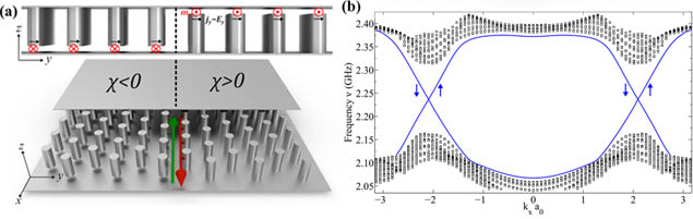
Figure 1. (a) The domain wall between two BMWs with reversed bianisotropy at the center. The 3D view of the domain wall has part of top metal plate removed to see the structure below. χ indicates the sign of bi-anisotropy in each domain (b) The corresponding PBS of the 1D supercell formed by two BMWs. In (b) black dots: bulk modes; blue lines: edge modes; arrows: effective spin of the edge modes [4].
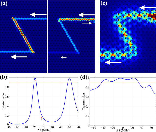
Figure 2. (a) The left inset shows the energy density of resonant-tunneling photonic defect mode through a zigzag channel between two trivial-gapped photonic crystal. The frequency of the mode indicated by red arrow at the peak in (b). The right inset shows the case of off-resonance. (b) Transmission spectrum of the defect mode with the frequency range in the band gap. (c) Reflection-free routing of the PTI edge mode. (d) Transmission spectrum of the PTI edge mode [4].
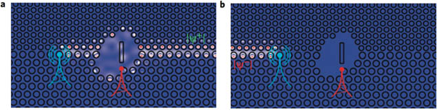
Figure 3. Non-obstructing large photon antennas due to spin-cloaking. Spin-cloaked electric-dipole antenna (indicated by the rectangular region) embedded into the cavity between topologically trivial and non-trivial metacrystals. a,b, The spin-polarized one-way transport of the spin-up ψe+ and spin-down ψe− edge modes avoiding a silent dipole antenna placed in the cavity [2].
Relevant publications:
[1] C. L. Kane and E. J. Mele, "Z2 Topological Order and the Quantum Spin Hall Effect," Phys. Rev. Lett. 95, 146802:1-4 (2005)
[2] A. B. Khanikaev, S. H. Mousavi, W.-K. Tse, M. Kargarian, A. H. MacDonald, G. Shvets, “Photonic Topological Insulators”, Nature Materials 12, 233–239 (2013). DOI: 10.1038/NMAT3520 (published online).
[3] J. D. Joannopoulos et al, Photonic Crystals 2nd ed, chap. 3, 4 (Princeton University Press, 2008)
[4] Ma, T., Khanikaev, A. B., Mousavi, S. H., Shvets, G., Topologically protected photonic transport in bi-anisotropic meta-waveguide, eprint arXiv:1401.1276 (2014)
